|
|
     aHR0cDovL2ZyZWVzaGlwLmNvLmty aHR0cDovL2ZyZWVzaGlwLmNvLmty
- 호환 오디오 및 비디오 장비 스타일: 전문 오디오 장비
- 브랜드 이름: OnifealiMajeson
- 원산지: 중국
Welcome to the MOFI-Acoustics store. In order to provide better shopping experience, let me clarify these informations to avoid unnecessary inconvinience:
1. All products in the store are not included: customs duties, customs clearance fees and tax. Without special requirements, we will declare them according to the price of the product.
2. We hope that you can understand the relevant taxation policies of your local customs. We do not accept your refusal for goods due to customs taxation issues; (in some countries, the platform has the option of pre-collecting tariffs).
3. In order not to affect your receipt of the goods, after purchasing the goods, please pay more attention to information such as emails, platform messages, etc. If there is any information about the unclear address or the logistics policy changes, we will notify you as soon as possible, and look forward to you reply.
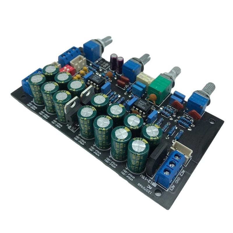
Printed Circuit Board Project
1、The PCBs sold in the store do not contain any components, and you should prepare them by yourself.
2、To complete this project, high level knowledge of electronics and rich experience in terms of soldering and testing are required.
3、Due to time zone and language communication restrictions, we can only provide limited technical support, and you need to solve problems by yourself.
4、 We do not provide information other than the product introduction page.
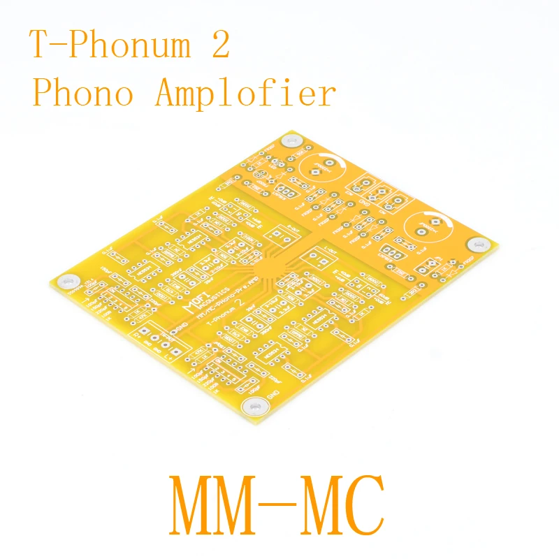
MOFI-Shiratori Phono Amplofier RIAA PCB Project
Tech highlights
1、 The circuit employs a particular two-stage RIAA equalization network, one active and one passive, which effectively solves the problems of accuracy, noise and input dynamics that typically arise using traditional active or passive networks.
2、 Some DIP switches on the board allow you to adjust the gain (MM and MC modes), the input capacity (to optimize the interface of the MM heads) and the input resistance (for the MC heads).
3、 The circuit employs a total of four individual operational amplifiers for audio applications, two for each channel.
4、 The two-stage RIAA network is low impedance to minimize thermal noise.
5、 This is driven by the first op-amp, which also provides a significant portion of the overall gain. The second op-amp provides the remaining necessary gain, which can be adjusted according to the output level of the cartridge used.
6、 The DIP switches can be activated according to various combinations to obtain 4 gain values, 8 capacitance values and 4 input resistance values.
7、 PCB Size: 100x120x1.6mm 1oz Cu, HASL with lead
Schematic & key point of debugging
PCB comes with component parameters for easy installation.
We only refer the schematic of the amplification part of the circuit. If you need full circuit parameter, please read the component value with the PCB by yourself; we do not provide additionally.
 
Instructions
Since the PCB holes are plated through, you only need to solder the parts from the bottom of the board. Do not drill or enlarge the holes because that would damage the through-plating.
Clean both sides of the blank PCB with paper towel and isopropyl alcohol or electronics flux remover, then solder the components to the board, starting with the lowest profile parts.
Make sure the correct part goes into each position on the circuit board. Measure each resistor with your multimeter to ensure it`s the proper value.
Clean up the solder flux residue from the board with isopropyl alcohol (or electronics flux remover) and a brush.
nspect all solder connections carefully, using a magnifying glass, to make sure there are no solder bridges or cold solder joints. Use a multimeter in ohms scale to check for short circuits. As a minimum, you should verify that the V+ DC are not shorted to ground, or to each other, and that the output pad isn`t shorted to ground. Correct any mistakes before proceeding to the next phase.
Parts list

|
|
|
|
|


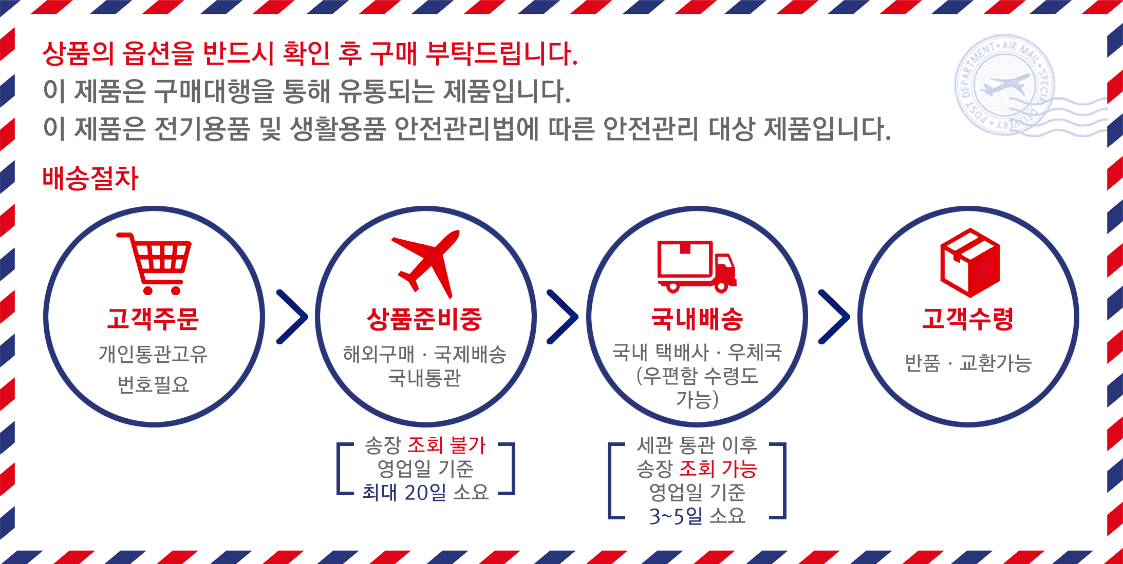
 배송기간
배송기간